
PCB Layout Design And Manufacturing
Jun 04, 2021, 13:06 IST
How to make PCB layout
We use printed circuit boards (PCB) for connecting electronic components using conductive tracks. This makes it possible to prototype electrical circuits and manufacture electronic products. Mass production of PCB-based electronic products is faster and more economical compared to products based on alternative wiring techniques. Therefore, we only need to make the PCB once, and we can manufacture a large number of PCBs at once.
When it comes to printed circuit boards, designing the layout is the most important part as it determines the placement of different components and their resulting roles in the desired product. This guide explains how to design a PCB layout and how to use it for PCB manufacturing.
First, we're going to take a look at some of the strategies commonly used in PCB layout design.
PCB layout design strategies
It is good practice to make a schematic of the circuit before you start designing the PCB. The schematic will serve as a blueprint for placing components and laying out the tracks on the circuit board. If you are using efficient PCB design software you can import this schematic and this will make the PCB design process relatively easier.
After you import this schematic into intelligent PCB design software, you can start placing components, wires, and footprints. Once we've done this, we can start designing the PCB layout.
You may find it difficult to design large circuits on a single layer PCB. This is because it is difficult to avoid intersections when routing tracks. You may need two or more layers with traces routed on multiple sides of the circuit board.
You can connect tracks on one layer to the other by a “via”. We know “via” as a copper-plated hole in a printed circuit board that electrically connects the bottom layer to the top layer. You can also connect the bottom and top tracks using the "through hole" of the deployed electronic components.

PCB design tools
There are numerous PCB layout design tools on the market today. You need to take a look at all important objectively and then choose the right tool that meets all your needs. Here are some of the layout design tools widely used in the PCB industry.
![]()
Altium Designer
Altium Designer is a full-featured most powerful PCB design tool in the market. It provides modern, end to end solution to PCB design engineers worldwide. Altium Designer is the most favourite design tools among engineers as it provides a unified design environment and uniting the design teams worldwide.
OrCAD PCB Designer
OrCAD PCB Designer has the most user-friendly UI and provides a comprehensive package to engineers to design Layout, schematics and footprints. It has a rich library of PCB footprints and circuit schematic symbols.
Zenit circuit board
It's a great software tool for creating great PCB layout designs. It is very easy to use and is very flexible. This CAD program enables its users to realize the projects in a very short time. ZenitPCB makes it possible to create the project by starting directly from the layout or by creating a schematic first.
Osmond PCB
Osmond PCB is a flexible PCB layout design tool. It includes a number of board layers and parts, virtually unlimited board sizes, support for build and continuous parts.
Express PCB
Easy to use and learn. This software makes it very easy to design PCB layouts even if the user is a beginner or has no previous knowledge.
Kicad
This tool helps create electronic schematic diagrams and PCB layouts. It supports PCB layout design with up to 16 layers.
Design Spark PCB
This PCB design tool has the highest accessibility as compared to other electronic design tools. It is very easy to use yet easier to learn. Experts use this tool to shorten turnaround times. This tool has a powerful design engine that makes it very useful for designing PCB layouts, boards, and schematics.
EasyEDA
EasyEDA is an online more powerful and easy to use PCB design tool that lets you import more than 1 million real-time updated components. This web-based design tool allows engineers and PCB designers to design, simulate share and discuss their designs both publically and privately.
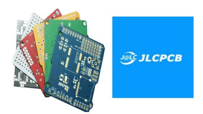
PCB Manufacturing
JLCPCB technology is a renowned name when it comes to PCB manufacturing. We have a very advanced setup to produce the premium quality PCB. If you have managed to come up with brilliant single-layer or multi-layer PCBs but can't realize your conceptualization then don't worry because we've got you covered. We provide the cheapest PCB prototypes starting from just $2. All you need to do is contact us and we'll take care of it from there. Hope to hear from you soon!
JLCPCB is a leading PCB manufacturer which provides the most efficient, cost-effective and reliable PCB solutions for your DIY, PCB prototypes and professional products. JLCPCB is committed to providing the most cost-effective and efficient PCB solutions to its customers. Its advanced PCB technology allows the manufacturing of high precision boards suitable for military, aerospace and industrial applications.


Related news
More from section
Advertisement